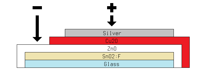
After a number of attempts to develop a graphite-based conductive paste, I decided to continue using silver paint for the time being. Compared to silver, graphite has poor conductivity, and it lacks the reflective properties which are beneficial for the back layer of a solar cell. Furthermore, I was using far less silver than I anticipated, so for now the cost is fairly insignificant. With that issue resolved, I moved on to optimization. For reference, a schematic diagram of the previous solar cell is shown below.
Since the tin oxide layer has already been optimized, the next step was to optimize the zinc oxide layer above it. This layer serves as the n-type semiconductor of the solar cell, and also acts as an adhesive primer for the subsequent copper oxide layer. Since I have no equipment to analyze the semiconducting properties of this layer, I generally focused on improving its adhesive properties. Previously I had used a solution of zinc chloride to prepare this layer, but this tended to produce an irregular, cracked film, which often resulted in large pinholes in the copper oxide layer above it. To resolve this issue, I returned to an earlier method for preparing zinc oxide using zinc acetate, and the resulting film was clear and uniform. Unfortunately it was also highly resistive, and solar cells made in this manner tended to produce very little current. To overcome this, I doped the solution with boric acid, just as I had done previously. Spraying a few milliliters of this solution on conductive glass heated to 400°C resulted in a transparent coating that was both conductive and adhesive enough for its intended purpose.
Having developed a suitable substrate, I then moved on to optimizing the copper oxide layer. Early experiments were poorly reproducible, with cells often having irregular coatings of uneven opacity and thickness. I eventually traced this back to the plating method, and discovered that plating at a constant voltage, rather than at a constant current, produced near-perfect results every time. When plating at a constant current, the glass substrate must be lowered into the plating bath before power is applied. Due to the highly alkaline nature of the bath, this tended to dissolve the zinc oxide layer. When plating at a constant voltage however, the power can be applied before the substrate is dipped into the bath, sidestepping this problem entirely. Furthermore, at a constant voltage, the cell will plate more slowly as the copper oxide becomes thicker, giving it time to grow evenly and ultimately producing a higher quality film.
With the ability to make reproducible copper oxide layers, I then set out to optimize the process. I started by modifying the plating bath's pH and temperature, since a number of research papers specified that increasing one or both of these variables had the tendency to improve the conductivity of the copper oxide. Unfortunately, beyond a pH of 11 or a temperature of 75°C, the bath becomes unstable and begins to precipitate copper oxide, quickly becoming muddy and unusable. For this reason, all further experiments were done at a pH of 10 and a temperature of 70°C. Next, I began varying the plating rate and duration, at which point I noticed an interesting phenomenon. No matter what values I chose for those two variables, I could not produce a solar cell with a short circuit current greater than 0.25mA/cm˛; however, the majority of the cells ended up very close to this value. If this were a characteristic of the material itself, I would expect the average and the absolute limit to be significantly different.
After thinking the problem over, I began to suspect that the current limiting factor was the contact resistance between the silver paint and the copper oxide layer. Since the copper oxide is made of microscopic crystals, and the silver paint is made of microscopic flakes, only point contacts connect the two. Between these points, the current is forced to travel sideways through the copper oxide layer until it finds the nearest silver flake. This is hardly optimal, since copper oxide is highly resistive. Ideally, a thin layer of silver could be deposited in a vacuum chamber to create a conformal coating over the entire surface of the copper oxide, but that would greatly increase the complexity of this project, which is unacceptable. Instead, I used copper sulfide.
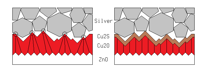
Copper (I) sulfide (Cu2S) is a highly-conductive p-type semiconductor, that can achieve near-metallic conductivity in very thin layers. Conveniently, such a layer is easily formed by dipping copper oxide in a dilute solution of sodium sulfide (Na2S). If the solution concentration and dipping time are carefully managed, the result is the structure shown above. The copper sulfide acts as an intermediate current collector between the copper oxide and the silver paint, and since it covers the entire surface area of the copper oxide, the current can take the shortest possible path through the most resistive layer of the cell.
Early experiments with this sulfiding process immediately doubled the current output of the cells I used it on, confirming my earilier suspicions about the nature of the limiting factor. Unfortunately the process also reduced the voltage output of the cells by almost 90%. I struggled with this for nearly a month, until I finally realized the nature of the problem. I had initially thought that the characteristics of the bulk copper oxide were being changed by its reaction with sulfur, and that this new composite material was inferior to the pure oxide. What was actually happening can be seen below.
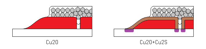
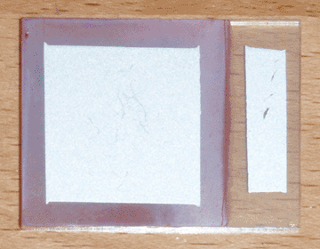
Since a layer of highly conductive copper sulfide was being formed on top of the copper oxide, short circuits were forming at the edges and pinholes. I immediately took an early test cell, used a razor to cut the edges off, and measured the voltage. It had greatly improved. Having solved the last remaining problem, I immediately made a new solar cell from scratch.
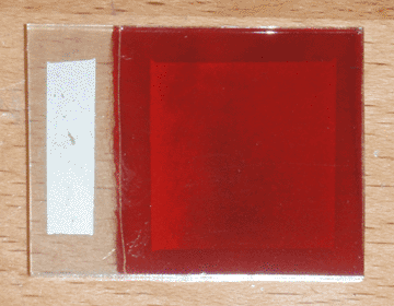
I began with a small ticket of conductive glass, on which I sprayed 3mL of 1M zinc acetate solution doped with 2% boron, at a temperature of 400°C on my graphite hot plate. I then plated a layer of copper oxide on the glass at a pH of 10 and a temperature of 70°C for 15 minutes, with an initial current of 3mA/cm˛. I then washed the cell with tap water, and dipped it for 3 seconds in a 0.2% solution of sodium sulfide (100mg in 50mL of distilled water) while it was still wet. I then let it hang in the air for 2 seconds to drip, then quickly swirled it in a half-liter beaker of tap water and rinsed it again afterward. I then let the cell sit in the warm air near my electric hot plate, and applied silver paint as soon as it was dry. Once painted, I returned the cell to the warm air to quickly cure the paint. Finally, I used a razor to separate the painted area from the edges of the cell. The finished product can be seen at the top of the page.
In direct sunlight, this cell has an open-circuit voltage of 205mV and a short-circuit current of 5.8mA. Initially the short circuit current was lower, but I found that squeezing the alligator clip on the conductive glass increased it, so I added a strip of silver paint to widen the contact area and eliminate the bottleneck. Interestingly, it is difficult to determine the active area of the cell; although the area under the silver paint is largely responsible for the bulk of the current, this area is extended somewhat by the highly conductive copper sulfide. In fact, the copper sulfide is so conductive, a single point probe can pick up nearly half a milliamp when touching outside of the painted area. That being the case, the conservative estimate for the current density is 0.93mA/cm˛ (for 6.25cm˛ of copper oxide), and the optimistic estimate is 1.70mA/cm˛ (for 3.42cm˛ of silver paint).
While this cell is certainly better than any I have made before, it is still only partially optimized. Having solved the contact resistance problem, I plan to revisit each layer of the cell and improve them to the extent that I can with the tools I have available. Specifically, I will attempt to improve the conductivity of the zinc and copper oxide layers, and I will optimize the sulfiding process to minimize the leakage current within the cell, which I believe is the source of the low open-circuit voltage. I also have some chemical modifications to the plating bath in mind, and may also return to my search for an alternative back contact material.